Motherboard Chipsets and Memory Map
(1) NOTE: This article is from 2008, close to the version 2.0 of UEFI.
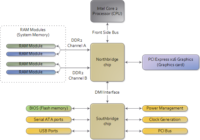
This shows that the CPU doesn't really know what the outside world is. It just uses its pins to connect to the outside world without caring what it is.
The motherboard has a front-side bus that connects the CPU to the northbridge chip and indirectly connects to the other parts. This bus is used when it needs to read or write to memory. CPU and the outside world communicate through 3 ways:
- Memory address space
- I/O address space
- Interrupts
It uses the pins to specify the physical address it wants to read and write, and the data to be written or received. The Intel Core 2 shown in the diagram above has 33 pins for physical memory address and 64 pins to send or receive data.
Thus data is transmitted in a 64-bit data path, and the chip can technically handle a physical address space of maximum 64 GiB. Physical address is not just for RAM, though it primarily is. It is also used for memory-mapped I/O devices like video cards PCI (Peripheral Component Interconnect) cards like scanners or SCSI, and even the flash memory that stores the BIOS.
The northcard reads the physical memory location and decides where to route it to via its memory address map. The file /proc/iomem shows the memory locations (DEBUG: (2)).
❯ sudo cat /proc/iomem
[sudo] password for resyfer:
00000000-00000fff : Reserved
00001000-0009efff : System RAM
0009f000-000fffff : Reserved
  000a0000-000bffff : PCI Bus 0000:00
  000f0000-000fffff : System ROM
00100000-5aaa2fff : System RAM
5aaa3000-5ab2bfff : Reserved
5ab2c000-5f72afff : System RAM
5f72b000-63510fff : Reserved
63511000-63d71fff : ACPI Non-volatile Storage
63d72000-63ffefff : ACPI Tables
63fff000-63ffffff : System RAM
64000000-67ffffff : Reserved
68700000-687fffff : Reserved
69000000-707fffff : Reserved
  6c800000-707fffff : Graphics Stolen Memory
70800000-bfffffff : PCI Bus 0000:00
  70800000-708fffff : PCI Bus 0000:02
    70800000-70803fff : 0000:02:00.0
    70804000-70804fff : 0000:02:00.0
      70804000-70804fff : r8169
  70900000-709fffff : PCI Bus 0000:01
    70900000-70903fff : 0000:01:00.0
      70900000-70903fff : nvme
  70a00000-70a01fff : 0000:00:17.0
    70a00000-70a01fff : ahci
  70a02000-70a02fff : 0000:00:1f.5
    70a02000-70a02fff : 0000:00:1f.5 0000:00:1f.5
  70a03000-70a037ff : 0000:00:17.0
    70a03000-70a037ff : ahci
  70a04000-70a040ff : 0000:00:17.0
    70a04000-70a040ff : ahci
c0000000-cfffffff : PCI ECAM 0000 [bus 00-ff]
fd000000-fd68ffff : pnp 00:06
fd690000-fd69ffff : INT34C5:00
  fd690000-fd69ffff : INT34C5:00 INT34C5:00
fd6a0000-fd6affff : INT34C5:00
  fd6a0000-fd6affff : INT34C5:00 INT34C5:00
fd6b0000-fd6cffff : pnp 00:06
fd6d0000-fd6dffff : INT34C5:00
  fd6d0000-fd6dffff : INT34C5:00 INT34C5:00
fd6e0000-fd6effff : INT34C5:00
  fd6e0000-fd6effff : INT34C5:00 INT34C5:00
fd6f0000-fdffffff : pnp 00:06
fe000000-fe01ffff : pnp 00:06
fe04c000-fe04ffff : pnp 00:06
fe050000-fe0affff : pnp 00:06
fe0d0000-fe0fffff : pnp 00:06
fe200000-fe7fffff : pnp 00:06
fec00000-fec003ff : IOAPIC 0
fed00000-fed003ff : HPET 0
  fed00000-fed003ff : PNP0103:00
fed20000-fed7ffff : Reserved
  fed40000-fed44fff : INTC6000:00
    fed40000-fed44fff : INTC6000:00
fed90000-fed90fff : dmar0
fed91000-fed91fff : dmar1
feda0000-feda0fff : pnp 00:05
feda1000-feda1fff : pnp 00:05
fedc0000-fedc7fff : pnp 00:05
fee00000-feefffff : pnp 00:05
ff000000-ffffffff : pnp 00:06
100000000-28f7fffff : System RAM
  178e00000-17a1fffff : Kernel code
  17a200000-17aff0fff : Kernel rodata
  17b000000-17b2a233f : Kernel data
  17bc78000-17c1fffff : Kernel bss
28f800000-28fffffff : RAM buffer
4000000000-7fffffffff : PCI Bus 0000:00
  4000000000-400fffffff : 0000:00:02.0
  4010000000-4016ffffff : 0000:00:02.0
  4017000000-4017000fff : 0000:00:15.0
    4017000000-40170001ff : lpss_dev
      4017000000-40170001ff : i2c_designware.0 lpss_dev
    4017000200-40170002ff : lpss_priv
    4017000800-4017000fff : idma64.0
      4017000800-4017000fff : idma64.0 idma64.0
  4017001000-4017001fff : 0000:00:15.1
    4017001000-40170011ff : lpss_dev
      4017001000-40170011ff : i2c_designware.1 lpss_dev
    4017001200-40170012ff : lpss_priv
    4017001800-4017001fff : idma64.1
      4017001800-4017001fff : idma64.1 idma64.1
  4020000000-40ffffffff : 0000:00:02.0
  6000000000-6000ffffff : 0000:00:02.0
  6001000000-60010fffff : 0000:00:1f.3
  6001100000-600111ffff : 0000:00:04.0
    6001100000-600111ffff : proc_thermal
  6001120000-600112ffff : 0000:00:14.0
    6001120000-600112ffff : xhci-hcd
  6001130000-6001137fff : 0000:00:0a.0
    6001134000-60011348ff : telem1
    6001136198-60011361a7 : intel_vsec.telemetry.0
    60011361a8-60011361b7 : intel_vsec.telemetry.0
  6001138000-600113bfff : 0000:00:1f.3
    6001138000-600113bfff : ICH HD audio
  600113c000-600113ffff : 0000:00:14.3
    600113c000-600113ffff : iwlwifi
  6001140000-6001143fff : 0000:00:14.2
  6001144000-60011440ff : 0000:00:1f.4
  6001145000-6001145fff : 0000:00:16.0
    6001145000-6001145fff : mei_me
  6001148000-6001148fff : 0000:00:14.2
This is the cause of the 3GB barrier(3) where 32-bit OSes are supposed to be compatible with 4 GB of memory, but that only refers to 4GB of physical memory space, not 4 GB RAM. There is a classic big hole in between around 640KB to 1MB and can be bigger due to video and PCI cards and often around the top 1 GB is mapped to devices. However, some had an extension to this.(4)
In my case, the first 4 MB are reserved (among some other sections) and is dependent on the motherboard and devices present. These are physical addresses that are used to write to the motherboard buses. Inside the CPU (like in the programs we write and run), the memory addresses are logical addresses, and need to be translated by the CPU to a physical address before accessing it through the bus.
There are two ways of accessing devices: memory-mapped I/O and port-mapped I/O. In memory-mapped I/O, you can continue using the same CPU instructions used to access main memory to access devices, and the motherboard will handle it for you. Port-mapped I/O requires special instructions from the CPU.(5)
Memory Translation from Logical to Physical
The translation of logical memory addresses to physical memory addresses is complex as it depends on the CPU mode (real mode, 32-bit protected mode, 64-bit protected mode). This mode decides how much of the physical address space can be accessed.
Real Mode
(6) It's a 20-bit addressing mode that provides unlimited direct to all physical address. No support for memory protection, multi-tasking or code-privileges. Before Intel's 80286, real mode was the only mode available. Post that, protected mode became a thing. 20-bit means 1 MB of address space.
64-bit Mode
A 64-bit mode can access memory wayyyyyyyyyyy larger than the current RAM sizes. Thus, it's possible to use the physical addresses above the total RAM to compensate for the physical address space lost to devices. This is called reclaiming the memory and is done through help from the chipset.
Interesting Read
This paper: (7).
References
- (1): https://web.archive.org/web/20180713151039/https://manybutfinite.com/post/motherboard-chipsets-memory-map/ (opens in a new tab)
- (2): https://unix.stackexchange.com/questions/358050/why-entries-in-my-proc-iomem-are-all-00000000-00000000 (opens in a new tab)
- (3): https://en.wikipedia.org/wiki/3_GB_barrier (opens in a new tab)
- (4): https://en.wikipedia.org/wiki/Physical_Address_Extension (opens in a new tab)
- (5): https://en.wikipedia.org/wiki/Memory-mapped_I/O_and_port-mapped_I/O (opens in a new tab)
- (6): https://en.wikipedia.org/wiki/Real_mode (opens in a new tab)
- (7): https://www.akkadia.org/drepper/cpumemory.pdf (opens in a new tab)
⌂ Home
MIT 2024 © resyfer.